
| Summary : |
![]()
DDR-II : How it works
From our LGA775 Review
The first visible difference of DDR2 -- its connector: Of an identical size to the old DDR modules, the number of pins, however, increased from 184 to 240. At the same time, the use of BGA packaging is now required, whereas it was seldom used in traditional DDR modules. Contrary to the change from SDR to DDR, the goal of the DDR2 is not to offer more bandwidth at a frequency equal to DDR1, but to enable a continued rise in frequency through improved signaling. Indeed, DDR2 will start where DDR stops officially, i.e. at 200 MHz (DDR400). The first chipsets such as the i9xx will support DDR2-400 (PC2-3200), as well as DDR2-533 (PC2-4300). Moreover, DDR2 brings other advantages in terms of evolution. So while DDR modules are limited to 1 GB, DDR2 should quickly allow 2GB and soon 4GB, and possibly 8GB modules...
- Function
Now let’s check out the differences between DDR and DDR2. The improvement modifications made by DDR2 vis-a-vis DDR1 are as follows:
- Frequencies of operation/Data Prefetch
- Addition of On-Die Termination
- OCD Calibration
- Increase in the number of banks
- Modification of latencies
- Adoption of BGA package
In short, a whole program which we will now study in detail starting from the bottom
- Frequencies of operation/Data Prefetch
Now let’s study the evolution in terms of frequencies of operation of SDRAM to DDR2:
| Let us start by speaking about traditional SDRAM. A memory module consists of three fundamental elements. The first is the group of memory cells called the "Memory Cell Array"; next are the input/output buffers (I/O Buffers); then the data bus. In the case of PC100 SDRAM, these three subsets all function at 100 MHz. That is to say the memory cell provides 1 bit every 10 ns to the I/O buffer which in turn sends it across the bus at a frequency of 100 million bits per second (100 MHz). As SDRAM uses a 64-bit wide bus, you get a bandwidth of (100*64)/8 = 800 MB/s. Simple. | 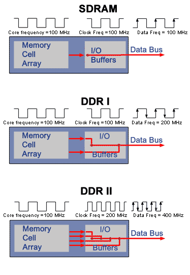 |
| With the evolution of SDRAM, the technology of that era limited the frequency of the memory cells to around 166 MHz. The goal then was to return to 100 MHz and to find other ways to exploit this frequency: DDR PC1600 was born. If the core frequency remains identical, it now returns 2 bits to each cycle, hence this is known as a 2-bit prefetch. However, in order for the I/O buffer to continue to work to 100 MHz, the idea of using both edges of the clock signal rather than the binary states was employed. In short, while remaining at 100 MHz, DDR makes it possible to transfer 200 million bits a second, that is to say a bandwidth of ((100*2)*64)/8 = 1600 MB/s. | |
| Reaching 200 MHz on DDR1, the memory arrays started to suffer. Solution? Return to 100 MHz, of course! But this time, to maintain the flow, it was necessary to double the frequency of the I/O buffers. DDR2 PC3200 thus uses an internal frequency of 100 MHz, these cells provide 4 bits per cycle to the I/O buffer which now functions at 200 MHz. The prefetch thus changes from 2 bits to 4 bits. In the end, on the data bus, you then get the same thing as with DDR (use of the rising and falling edges of the signal), but at double the frequency. So the data rate for a base frequency of 100 MHz is ((100*4)*64)/8 = 3200 MB/s. |
In short, all this is based on a very significant modification, which is the prefetch data. How is it possible in an array of memory cells to provide 2 or 4 bits per cycle? Simply by dividing it. If in the case of the SDRAM, the memory array consisted of a single physical block, it is divided (physically) into two in the case of DDR and into four for DDR2:
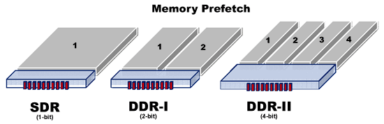
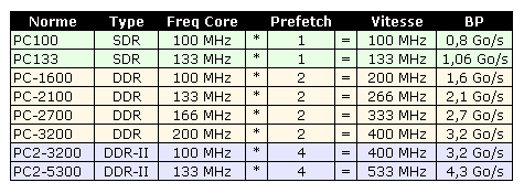
It should be noted that the physical spacing follows an increase in the die size of approximately 3%, which is not negligible (but not catastrophic either) for production. Now let’s look at the bandwidth obtained with the various generations of memory and the internal core frequency:
The interest in returning to a 100 MHz core frequency is two-fold. Firstly, this makes it possible to go up in frequency since it is now known that the cores can support more than 200 MHz, moreover, this improves the yield considerably since producing a 100 MHz memory array is relatively easy. Then, the low operating frequency allows lower power consumption, which is not negligible for very high density memories.
Now let’s continue this study with the process of on-die termination:
- Ajout de terminaisons On Die
Another significant feature of DDR2 is On-Die Termination. Similar to SCSI peripherals, the end of the "chain" of memory modules must be terminated in order to avoid the phenomena of signal reverberations, which can interfere with critical memory signals. Until now, these terminations were positioned on the motherboard and ended the chain. In the case of the DDR2, these terminations are now included inside the chip die and can be activated on demand (only the last module must be terminated). Let’s examine that more closely:
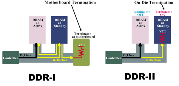
In the case of DDR1 the phenomena of reverberations are an issue at higher frequencies, whereas with DDR2 they are much smaller. This mainly makes it possible to increase the reliability of the signal and thus the maximum frequencies possible in DDR2. In analyzing memory signals, the reliability of the signal is often measured in an electronic eye signal diagram. The Eye is the part of the effective signal, which will be read. The more it is large and wide (one says "open"), the more the signal will be of good quality. Here is a typical example of an Eye:
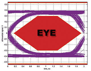
The red rhombus in the middle symbolizes the effective field of the signal. To return to our discussion on ODT (One Die Termination), it is used to increase the eye and thus the effective field of the signal. In the case of DDR2, you can see in the comparative measurements taken below that the result is very encouraging:
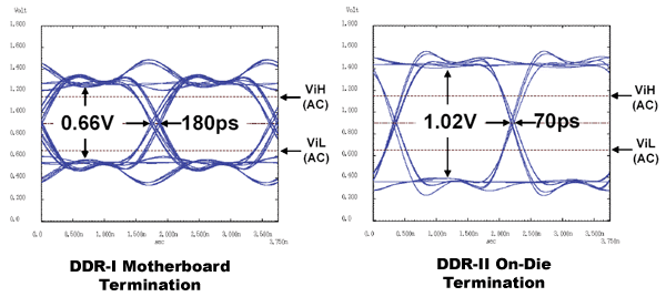
By increasing the voltage range and by decreasing the transitions from state (180 ps for DDR1, 70 ps for DDR2), the internal terminations play their roles very well here. This significant improvement first makes it possible to scale up the frequency more easily, but also allows a reduction in the price of the motherboard. The many resistor-capacitor networks used for the memory terminations are no longer necessary.
- Other architectural modifications
Now let’s look at the other architectural improvements made in DDR2. We should start by discussing the OCD or Off Chip Driver Calibration. The truth is, there’s no easy way to explain this technology. In fact, to simplify to the extreme, the OCD Calibration makes it possible to prevent a shift between the various clock signals by adjusting the impedance buffer. The goal being that two reversed signals cross exactly in their centers as one can see on the graph below:
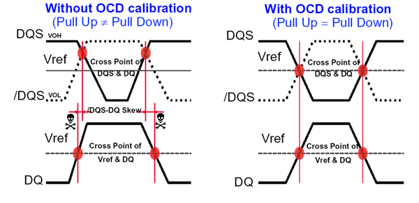
The transitions are not perfectly synchronous, and this shift increases the time of transition and therefore, the size of the eye we discussed above decreases. It should be noted that the adjustment is made via the BIOS and the chipset at the time of bootup.
Another interesting point to note, the management of the chips’ internal banks. If DDR1 had a 4-bank architecture, i.e. 4 sections of independent memory inside each chip, the DDR2 will have 8 internal banks, which means the total size of chip will reach 1 Gbits and more. So the performance should be higher with such chips. Indeed, the greater the number of banks (especially on very high capacity chips), the greater the throughput can be increased.
The last point to be developed is the evolution of timings. Concerning CAS, the first values seen were 5 and going forward, the only official values available will be 3, 4 or 5. The majority of the other known parameters (RAS-to-CAS et RAS Precharge) remain unchanged with a range from 3 to 5. As for RAS, the range remains between 3 and 15. It should be noted that, concerning Write Latency, it is henceforth equal to Read_Latency - 1 whereas it was 1 CLK on DDR1 regardless of the state of Read_Latency. The average
- Transition to FBGA packaging
Indeed, where DDR modules used the traditional TSOP extensively, DDR2 modules will be available only FBGA (Fine Ball Grid Array) format. This packaging indeed has much better electrical and thermal characteristics than TSOP:
It also allows advanced techniques of Die Stacking making it possible to combine several dice into the same package in order to reach greater densities. Let’s look at, for example, the ball-out of an Infineon x8 memory chip:
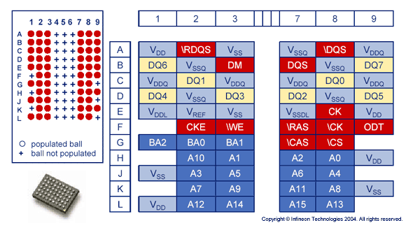
As seen here, in the dead center of the chip, the data pins are well isolated from the others, which eliminates part of the cross-talk of the TSOP on the module PCB. This type of packaging was essential for the data rates that were planned for DDR2.
- Evolution de la DDR-II
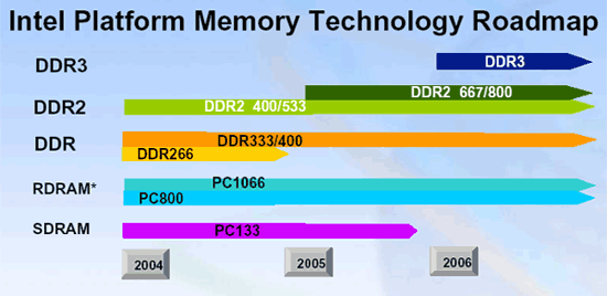
To date, only DDR2-400 and DDR2-533 standards are validated. If, with the nod from INTEL, the move to DDR2-667 will not pose much of a problem, it would seem that DR2-800 will not be available for at least a year and a half. DDR2-667 support is currently expected in the LakePort chipset, planned for Q2' 05. DDR3, also on the roadmap, will not be a mass memory before 2007.
In short, as we saw, DDR2 makes many technical improvements to the first generation. However, the beginnings at 400 and 533 MHz only allow a glimpse of the potential of this memory. Indeed, at these frequencies, the weak timings necessary to get the increase in frequency are likely to offset the gains in performance, we will examine with the Corsair DDR2-667 modules.